1. Introduction
RT6204 is a flexible buck converter for wide input
and output voltage range applications. It can be used with input voltages
from 5.2V up to 60V and the output can be adjusted from 0.8V up to 50V,
delivering up to 0.5A output currents. Chapter 2 provides an overview of
the application component selection and design considerations. Chapters
3, 4, 5 and 6 each describe a design with specific VIN/VOUT
condition from low 1.2V MCU supply to industrial supply providing 24V output.
2. RT6204 general design guidelines
The RT6204 application schematic is shown in figure
1. RT6204 is a current mode converter with external compensation and external
soft-start. The converter has both integrated high-side MOSFET switch and
synchronous rectifier switch. The output can be set via a simple resistor
divider. Current mode control with external compensation makes it possible
to tune the converter control loop for a wide range of output capacitors,
from low ESR ceramic types to aluminum electrolytic capacitors. This gives
the designer the freedom to choose the most suitable and cost effective
components for any output voltage application.
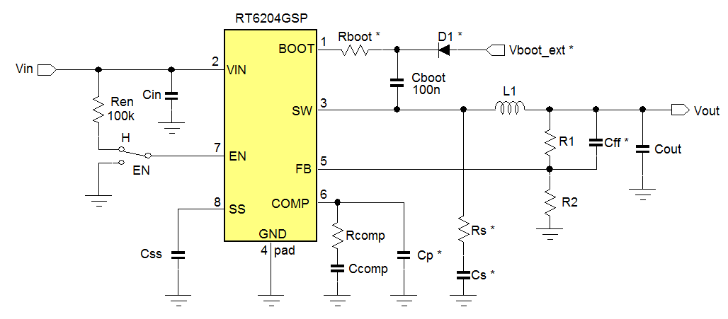
Figure 1
The following guidelines can be used to calculate the
various application components:
· Input
and output voltage considerations:
The RT6204 output voltage can be adjusted from 0.8V
to 50V by means of R1 and R2:

The impedance of the feedback network is not critical,
but it is recommended to avoid too high resistor values to reduce sensitivity
to noise. It is recommended to set R2 between 10kΩ ~ 30kΩ.
RT6204 has a low minimum on time of 90nsec, achieving
minimum duty-cycle in CCM mode of 90nsec ‧ 350kHz = 3.15%. It should be noted
that running the converter close to its minimum on time will influence output
ripple and over-current protection behavior. This is explained in chapter
3.
When operating RT6204 in high duty-cycles exceeding
65%, the external bootstrap supply via D1 should be added. The external
bootstrap supply is recommended to be around 3.3~3.8V. (Below 3.5V D1 should
preferably be a Schottky diode)
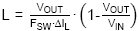
· For Inductor value of L1 there are two main criteria that need to be considered: Inductor current ripple and slope compensation. For applications with duty-cycle
lower than 50%, the inductor can be calculated to provide a ripple current
of 30% of the IC 0.5A rated current (ΔIL = 150mA):

· In applications
where the duty-cycle can exceed 50%, the inductor current falling slope
dI/dt also needs to fit the converter internal slope compensation: L1 value
needs to fulfill the following criteria:
 µH
µH
· For output
capacitor selection, there are several considerations:
a. Output ripple in CCM mode
Output ripple in CCM mode can be calculated from

The CCM mode inductor ripple can be calculated from:

When using ceramic output capacitors in these low
voltage supplies, output ripple voltage in CCM mode will be small.
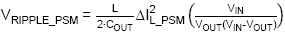
b. Output ripple in PSM mode
Output ripple in PSM mode will depend on the peak
current in PSM mode and the load current. The worst case condition will
happen at zero load:

RT6204 will regulate the inductor peak current in
PSM mode around 150mA but there is around 80nsec propagation delay, so at
high VIN and low VOUT the peak current will increase.
PSM output voltage ripple will always be higher than CCM ripple.
c. Voltage sag during load transients
The voltage sag during a load transient in CCM mode
depends on the load step, control loop speed and output capacitor. An approximate
formula for voltage sag during a fast load step is shown below:

where ΔISTEP is the load step amplitude
and FBW is the converter control bandwidth. Note that load step
transitions between PSM and CCM mode operation will show higher voltage
sag. Converter bandwidth is normally set around 1/10 of the switching frequency,
except when using electrolytic capacitors: The ESR variation over temperature
will require lower bandwidth setting to guarantee stable operation over
the full temperature range. The converter bandwidth can be set via compensation
resistor RCOMP.
· Input capacitor considerations
The input capacitor provides the high frequency
switching current peaks of the converter. The input capacitor should be
chosen to provide adequate filtering of the converter input, to minimize
the VIN high frequency ripple. Low ESR ceramic capacitors should
be placed close to the converter VIN and GND pins. At high input voltages,
ceramic capacitors will have severely reduced capacitance, which should
be considered when calculating the input ripple voltage. The peak-peak input
ripple voltage can be approximated by:
 where CIN is the capacitance at the DC input voltage.
You will normally need at least 1µF capacitance
and 100V rating, which will require 0805 or 1206 size MLCCs.
Another consideration for the input capacitor is
its RMS current rating:
 The maximum RMS current will happen when VOUT is 50% of VIN.
For the RT6204 maximum load current of 0.5A, the
maximum RSM current in the input capacitor will be 0.25A. This value is
normally not critical for ceramic capacitors with 0805 or 1206 size.
If the converter requires hot-plugging into live
input supplies, it is recommended to add a small electrolytic capacitor
in parallel with the ceramic input capacitor.
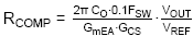
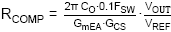
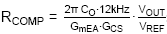
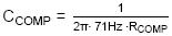
· Calculation of compensation components.
The RT6204 compensation can use standard current
mode type II compensation. The below simple formulas can be used:
The compensator gain is set by RCOMP,
and the value is calculated to provide a suitable converter crossover frequency
(FC around 0.1 ‧ FSW) with sufficient phase
margin.

Note that electrolytic output capacitors will require
lower bandwidth, see chapter 5.
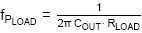
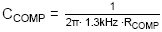
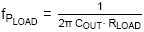
The value of CCOMP is selected to set
the compensation zero
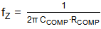 a bit below the converter load pole
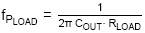 where RLOAD = VOUT/0.5A.
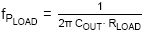
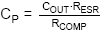
The value for CP is chosen to set the
high frequency pole at the output capacitor ESR zero:

When ceramic output capacitors are used, the ESR
zero will lie at very high frequencies, above the converter switching frequency.
For low VOUT applications with ceramic output capacitors, CP
can be omitted.
The feed-forward capacitor Cff is normally not needed
for improving control loop response. But some small Cff capacitor can sometimes
improve the PSM operation; by injecting some extra ripple on the FB pin
double pulsing can be reduced. This can be tested case by case.
· The soft-start
capacitor sets the time tSS from EN high to VOUT reaching
its final value which is defined by
 .
CSS is the value of the soft-start capacitor and ISS
is the soft-start current (typically 6µA). VOUT starts
rising when the VSS ramp passes 0.3V, and ends when VSS
ramp passes 1.1V.
.
CSS is the value of the soft-start capacitor and ISS
is the soft-start current (typically 6µA). VOUT starts
rising when the VSS ramp passes 0.3V, and ends when VSS
ramp passes 1.1V.
The VOUT rise time can therefore be calculated
by:
 .
.
Supplies with high output voltage and/or large value
output capacitors should use sufficient soft-start time to avoid high inrush
currents.
· The converter
can be enabled by pulling high the EN pin. The EN logic high level is typically
1.25V. There is a 1µA pull down current on EN. For automatic start-up
when VIN is applied, the EN pin can be connected with a 100k
pull-up resistor to VIN. The EN pin is 60V tolerant.
3. First Example application: 1.2V output
In this first example we will design a converter
with a fixed 1.2V output with a wide input voltage range.
· Maximum
input voltage: Based on minimum on time, the maximum input voltage for 1.2V
output will be 1.2/0.0315 = 38V. In this 1.2V example we will examine how
the minimum on time will influence output ripple and over-current protection
performance.
· Feedback
network: use
 to select R1 and R2: In this case we choose R1 = 7.5k and R2 = 15k which
will give exactly 1.2V output.
to select R1 and R2: In this case we choose R1 = 7.5k and R2 = 15k which
will give exactly 1.2V output.
· Inductor
value: For this 1.2 application, the duty-cycle will never reach 50%, so
slope compensation is not critical in this case. Therefore, the inductor
calculation can be purely based on ripple current.
Using VIN = 38V, and current ripple of
0.3 ‧ 0.5A=0.15A: using
 we find L = 22.1µH.
At max 0.5A load, the inductor peak current will
be (1+0.15) ‧ 0.5A = 0.575A. Normally the saturation current is chosen at
least 10% higher than the maximum peak current, so Isat should be > 0.63A.
For this example a Taiyo-Yuden NR6020T 22µH with Isat of 1A was chosen.
· For output
capacitor selection, we use the PSM ripple as selection criteria:
First the PSM peak current is estimated: With VIN
= 38V, VOUT = 1.2V, L = 22µH, the inductor current rising
slope is
(38-1.2)/22µH = 1.67A/µsec. 80nsec propagation
delay will result in 0.133A current increase. The PSM peak current will
therefore be around 280mA. For 1.2V output supply, we will use low ESR ceramic
capacitors. The capacitor ESR can therefore be neglected, and the PSM ripple
formula can be simplified:
 .
.
A worst case PSM ripple of 50mVpp requires 15.7µF
capacitance. For this example two 10µF/16V 0805 X5R size MLCC output
capacitors were selected: Murata GRM21BR61C106KE. The MLCC capacitance drop
due to 1.2V dc bias voltage is very low and can be neglected. But MLCC capacitance
is normally rated at an AC voltage of around 0.5Vrms. The capacitance will
drop at lower AC RMS voltage. For this low voltage ripple application, a 27%
capacitance drop must be considered. For more details on MLCC capacitor
behavior, please see
http://ds.murata.com/software/simsurfing/en-us/
The total effective output capacitance becomes ~15µF
output capacitance, which is used for further calculations.
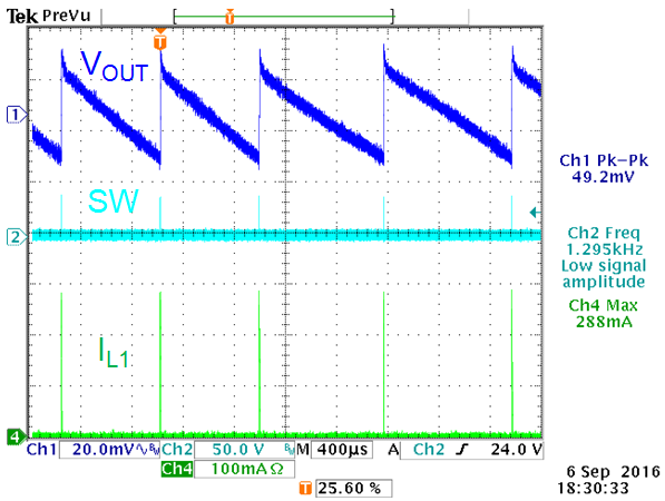
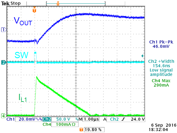
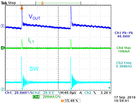
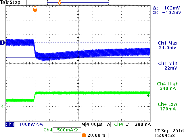
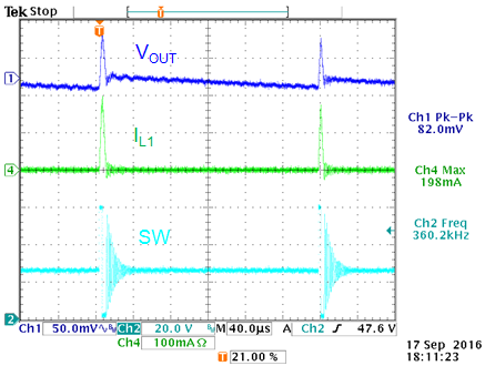
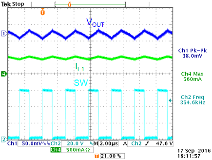
Measurements of the output ripple in PSM mode are
shown in the figure 2 below: L1 = 22µH, COUT_eff = 15µF
|
VIN = 38V, VOUT =
1.2V, 1mA load
|
PSM ripple with 15µF capacitance is
46mVpp.
|
|
|
|
Figure 2
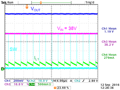
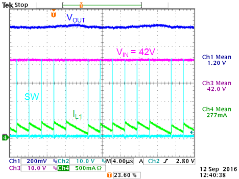
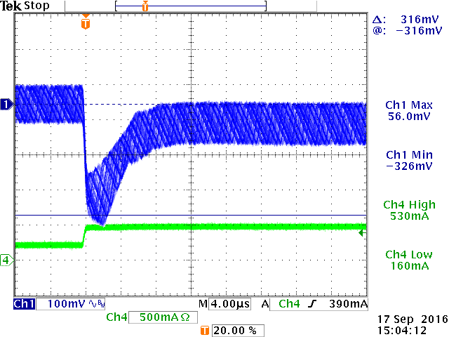
The effect of minimum ON time limit at high VIN
is shown in the figure 3 below: (VOUT = 1.2V, 0.28A load)
|
VIN = 38V: Just full PWM, no
pulse skipping
|
VIN = 42V: min ON time limit reached,
pulse skipping
|
|
|
|
Figure 3
When the minimum ON time is reached in high VIN
low VOUT applications, the converter will start skipping pulses
to maintain regulated output. This pulse skipping will result in higher
output voltage ripple.
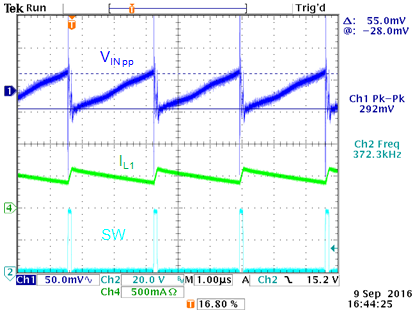
· For the
input capacitor selection, the maximum allowed input ripple needs to be
considered. The input capacitor also needs to have sufficient voltage rating.
For 40V input range, a capacitor having least 60V voltage rating needs to
be used. This normally means a ceramic capacitor with 100V rating.
According
 with 0.5A load current, 38V input and 1.2V output, 1µF of input capacitance
means that the input ripple will be around 44mV ripple. It should be noted
that this ripple does not include high frequency ringing due to capacitor
ESL and layout ESL.
with 0.5A load current, 38V input and 1.2V output, 1µF of input capacitance
means that the input ripple will be around 44mV ripple. It should be noted
that this ripple does not include high frequency ringing due to capacitor
ESL and layout ESL.
In this example we used a small 100nF/100V 0603
X7R capacitor (Murata GRM188R72A104KA35) in parallel with a 2.2µF/100V
1206 X7R capacitor (Murata GRM31CR72A225KA73) which has an effective capacitance
of 1.1µF at 38Vdc.
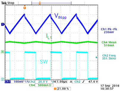
|
|
Figure 4 shows the input ripple voltage
measurement at 38V input and 0.5A load current.
The ripple voltage shows a saw-tooth with
55mVpp amplitude, but there is also considerable high frequency
noise present, due to parasitic ESL. To avoid this high frequency
noise entering the input power lines, it is recommended adding additional
filtering by means of a high frequency bead and extra capacitance.
The worst case RMS current in the input
capacitor for this application happens at the lowest input voltage
(5.2V), and will be around 0.2A. This will not be a problem for
the selected input capacitors.
|
|
Figure 4
|
|
· Calculation
of compensation components.
For the compensation component calculations we will
use the formulas as given in chapter 2. For the output capacitance we use
COUT_eff =15µF.
 : With GmEA = 970µA/V, GCS = 0.9A/V and COUT_eff
= 15µF: RCOMP becomes 5.7kΩ
: With GmEA = 970µA/V, GCS = 0.9A/V and COUT_eff
= 15µF: RCOMP becomes 5.7kΩ
We will choose 5.6kΩ
The converter load pole
 lies at 4.4kHz.
 = 6.4nF
We will choose 6.8nF.
The ceramic output capacitors will have a combined
ESR of 2.5mΩ. The ESR zero lies at 4.2MHz. CP can be omitted.
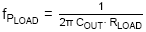
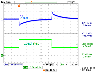
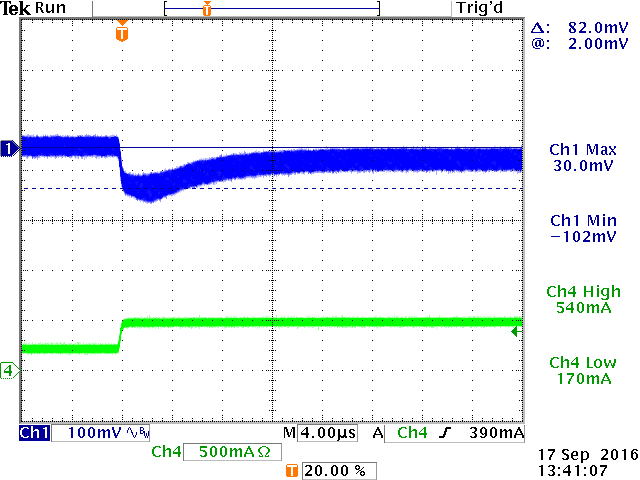
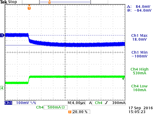
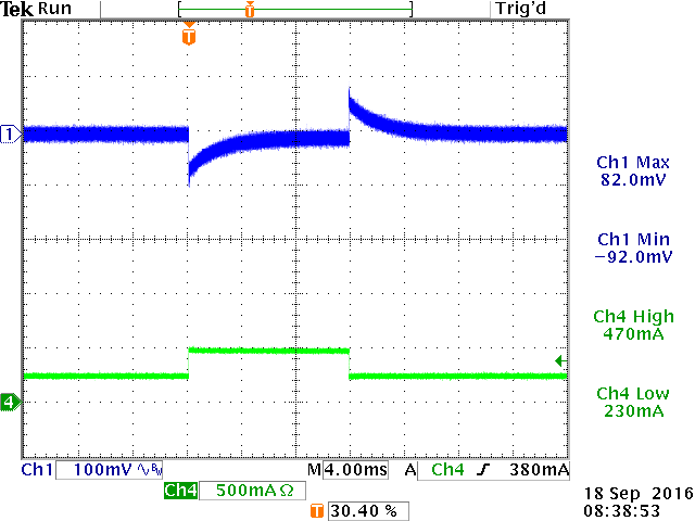
Converter stability was checked by means of fast
load step, see figure 5.
|
|
Fast load step at 24V input shows stable
performance without ringing.
Converter sag at 250mA load step shows 74mV
|
|
Figure 5
|
|
· The soft-start
capacitor sets the time tSS from EN high to VOUT reaching
its final value which is defined by
 .
CSS is the value of the soft-start capacitor and ISS
is the soft-start current (typically 6µA).
.
CSS is the value of the soft-start capacitor and ISS
is the soft-start current (typically 6µA).
For the 1.2V application with relatively small output
capacitors, inrush current is not critical. CSS = 10nF gives
a total start-up time of 1.83msec and VOUT rise time of 1.3msec.
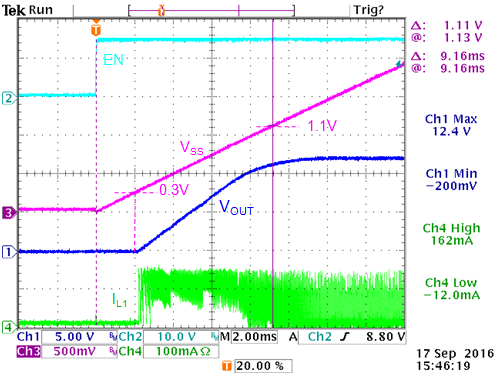
|
|
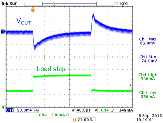
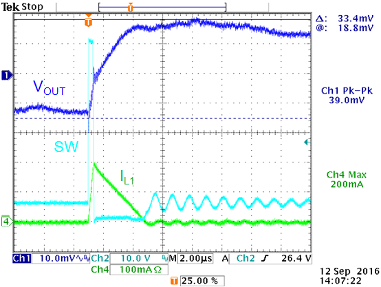
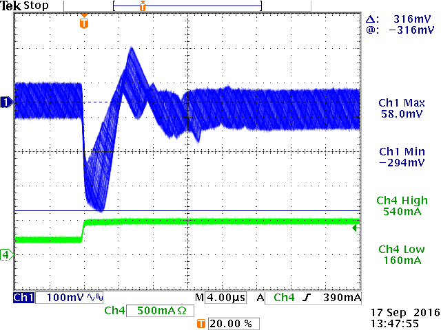
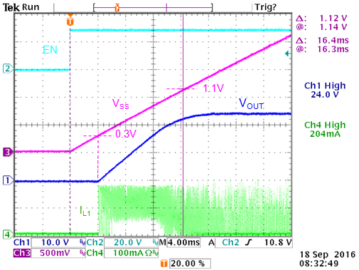
Figure 6 shows the soft-start behavior:
When EN goes high, the soft-start ramp starts rising. The converter
starts switching when the soft-start ramp passes 0.3V and VOUT
rises. Switching frequency gradually increases as VOUT
increases.
When the soft-start ramp reaches 1.1V, the
converter output reaches its final value.
|
|
Figure 6
|
|
· Over-current
protection behavior:
RT6204 has a cycle by cycle peak current limiting
circuit that uses the high side MOSFET current sense. When the converter
output loading is increased, at some point the peak current limit will be
reached: the protection circuit will then reduce the high side MOSFET on
time to avoid further current rise.
|
|
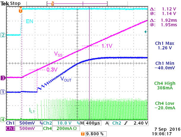
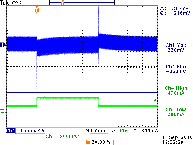
Figure 7 shows the current limit measurement
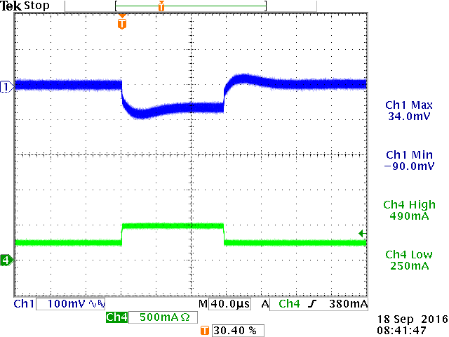
at VIN = 20V: When the inductor current reaches 950mA,
the duty-cycle is reduced and VOUT starts to drop. The
over current protection level of this 20V – 1.2V application is
slightly higher than the datasheet OCP level due to the current
sense propagation delay: (20-1.2)/22µH = 0.85A/µsec.
80nsec propagation delay will result in 0.068A current increase.
When VOUT drops below the output
under voltage protection (UVP level is 50% of VOUT),
the converter shuts down, and an automatic soft-start cycle is initiated.
|
|
Figure 7
|
|
When the RT6204 converter is operating in high input
voltage and low output voltage conditions and is subjected to overload situations,
it is important to make sure that the converter’s minimum on-time does not
prevent the current limit from operating properly. In minimum on time operation
mode and overload condition, the converter will operate at the minimum duty
and the output voltage will remain at whatever voltage that duty naturally
produces. In this overloaded state the inductor current is no longer controlled
and depends mainly on the load current, which eventually becomes high enough
for the MOSFET and inductor component voltage drops to increase enough to
allow VOUT to reach 50% and trigger UVP protection.
|
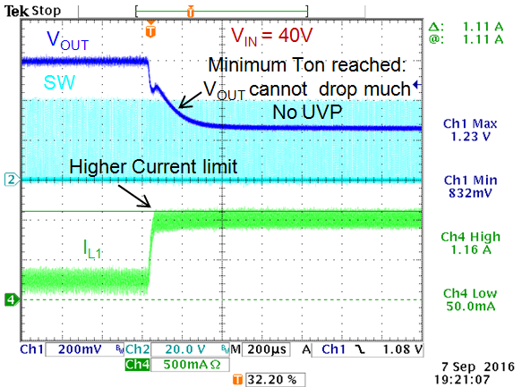
|
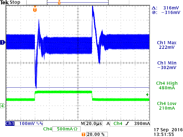
Figure 8 shows the current limit measurement
at VIN = 40V: Due to propagation delay, the OC level
now lies around 1.1A. The converter tries to reduce duty-cycle,
but it is operating close to its minimum TON time. It can be seen
that VOUT cannot drop much more and gets “stuck” around
830mV. The UVP level cannot be reached and the converter keeps operating
in this maximum overload condition.
When the converter load is further increased,
the inductor current can actually increase beyond the over current
limit. Any VOUT drop will now be caused by Rdson and
inductor DCR drop, which may still trigger UVP protection.
|
|
Figure 8
|
|
When the RT6204 converter is operating in high input
voltage and low output voltage conditions in combination with overload situations,
it is important to check the minimum on time limitations.
The complete 1.2V application is shown in figure
9.
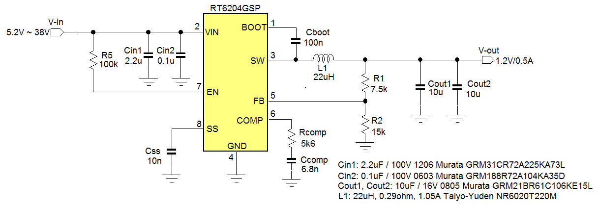
Figure 9
4. Second Example application: 5V output
The second example explains the converter with a
fixed 5V output with a wide input voltage range.
· The maximum
input voltage for this case is limited by the RT6204 60V maximum voltage
rating: 5/60 = 8.3%, which is much larger than the RT6204 minimum duty-cycle
of 3.15%. If the input supply can be lower than 7.5V, the duty-cycle will
be higher than 65%, and the external bootstrap diode needs to be implemented.
· Feedback
network: use
 to select R1 and R2: In this case we choose R1 = 43k and R2 = 8.2k which
will give 4.995V output.
to select R1 and R2: In this case we choose R1 = 43k and R2 = 8.2k which
will give 4.995V output.
· Inductor
value: For this 5V application, the duty-cycle can exceed 50% when VIN
is lower than 10V: for wide VIN applications, the effect of slope
compensation on the minimum required inductance needs to be considered.
The slope compensation criteria
 requires an inductor greater than 83µH.
Inductor calculation based on 30% current ripple
at 60V input using
 will give L = 87.3µH. In this example we will use 100µH. The
selected inductor is a 100µH Wuerth Electronic 744066101 shielded
inductor with a 1.2A saturation current and 0.255Ω resistance.
will give L = 87.3µH. In this example we will use 100µH. The
selected inductor is a 100µH Wuerth Electronic 744066101 shielded
inductor with a 1.2A saturation current and 0.255Ω resistance.
· For output
capacitor selection, we use the PSM ripple as selection criteria:
First the PSM peak current is estimated: With VIN
= 60V, VOUT = 5V, L = 100µH, the inductor current rising
slope is
(60-5)/100µH = 0.55A/µsec. 80nsec propagation delay
will result in 0.044A current increase. The PSM max peak current will therefore
be around 194mA. Note that at lower VIN, peak current increase
due to propagation delay is very small, and the nominal 150mA PSM peak current
can be used. For this 5V output supply, we will use low ESR ceramic capacitors.
The capacitor ESR can therefore be neglected, and the PSM ripple formula
will be:
At 60V input, a PSM ripple of 50mVpp requires around
9µF capacitance. For this example we used two 10µF/25V X5R 1206
size MLCC output capacitors, each having an effective capacitance of 6µF
at 5Vdc bias and low AC ripple voltage. The effective capacitance becomes
12µF output capacitance, which is used for further calculations.
Calculated PSM ripple at 60V input with 12µF output capacitance will
be 37mVpp.
|
|
Figure 10 shows the zero load PSM ripple
for the 5V application with 60V input and 12µF effective output
capacitance. PSM peak current and 39mVpp output ripple matches the
calculated values quite well.
|
|
Figure 10
|
|
· For the
input capacitor selection, the maximum allowed input ripple needs to be
considered. The input capacitor also needs to have sufficient voltage rating.
For 60V input range, a capacitor having least 90V voltage rating needs to
be used. This normally means a ceramic capacitor with 100V rating.
According
 with 0.5A load current, 60V input and 5V output, 1µF of input capacitance
gives input ripple will be around 110mV ripple. It should be noted that
this ripple does not include high frequency ringing due to capacitor ESL
and layout ESL.
with 0.5A load current, 60V input and 5V output, 1µF of input capacitance
gives input ripple will be around 110mV ripple. It should be noted that
this ripple does not include high frequency ringing due to capacitor ESL
and layout ESL.
In this example we used a small 100nF/100V 0603
X7R capacitor (Murata GRM188R72A104KA35) in parallel with two pieces 2.2µF/100V
1206 X7R capacitor (Murata GRM31CR72A225KA73) each having an effective capacitance
of 0.7µF at 60Vdc. The total combination of 1.5µF would give
around 78mVpp calculated input ripple at 60Vdc input and 0.5A load.
The worst case RMS current in the input capacitor
in this 5V application will happen when VIN is 10V and the load
is 0.5A. The maximum RMS current will be 0.25A; this will not be a problem
for the selected input capacitors.
|
|
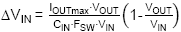
Figure 11 shows the actual input ripple
measurement, which shows 79mV saw-tooth input ripple. Additional
high frequency noise is due to parasitic inductance.
|
|
Figure 11
|
|
· Calculation
of compensation components.
For the compensation component calculations we will
use the formulas as given in chapter 2. For the output capacitance we use
COUT_eff = 12µF.
 : With GmEA = 970µA/V, GCS = 0.9A/V and COUT_eff
= 12µF: RCOMP becomes 19kΩ. We will choose 18kΩ.
: With GmEA = 970µA/V, GCS = 0.9A/V and COUT_eff
= 12µF: RCOMP becomes 19kΩ. We will choose 18kΩ.
The converter load pole
 lies at 1.3kHz.
 = 6.8nF.
The ceramic output capacitors will have a combined
ESR of 2.5mΩ. The ESR zero lies at 5.3MHz. CP calculation
based on this ESR zero will be 1.6pF. But for higher output voltage application
with larger duty-cycle variation, a larger value of CP is recommended.
The datasheet recommended value of 47pF sets the compensator pole at 188kHz,
which makes the converter operate more stable at higher duty-cycles at the
expense of slightly lower overall phase margin.
|
|
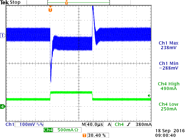
Figure 12 shows the output response with
a fast load step from 200mA to 420mA. (Converter operating in CCM
mode with an input voltage of 50V)
The response is stable without ringing.
Converter voltage sag at 220mA load step shows 90mV.
|
|
Figure 12
|
|
· For this
5V application with relatively small output capacitance, inrush current
is not critical. The same 10nF soft-start capacitance as used for 1.2V application
can be used, which gives total start-up time of 1.83msec based on:
 .
VOUT rise time from zero to 5V will be 1.3msec.
.
VOUT rise time from zero to 5V will be 1.3msec.
· External
Bootstrap capacitor charging circuit.
If the converter input can be lower than 7.5V, the
external bootstrap supply is needed. The optimal value for this bootstrap
supply is around 3.3V: Higher values like 5V can lead to too strong high-side
MOSFET drive which can lead to noise and unstable switching at certain conditions.
The 3.3V bootstrap supply can be derived from the 5V output by using a zener
voltage clamp. The average current that the external bootstrap circuit needs
to supply is low, around 1mA max. The peak current in D1 is around 40mA
max, and a small buffer capacitor can be used to supply this current.
For the external bootstrap supply we will use zener
clamp circuit: See figure 13.
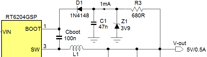
Figure 13
To minimize the power needed for the circuit, the
zener current is kept low, around 1mA. To compensate for the lower zener
knee voltage at low current, a higher voltage zener diode is chosen, Vishay
BZX384C3V9. Using a 680Ω bias resistor, at 5V output and 1mA bootstrap
charging current, the current in the zener will be around 1.5mA with a zener
clamping voltage of 3.5V. The total power dissipation in R3 is 2.5mA2 ‧ 680Ω
= 4.25mW, so a small size SMD resistor can be used. The 47nF capacitor provides
sufficient buffer for the 40mA D1 current pulses.
When the converter goes into max duty-cycle dropout
mode, VOUT will reduce and the external boot supply will drop
to around 3.2V. This is still sufficient to drive the bootstrap supply.
The figure 14 below shows the 5V converter operation
at maximum load when VIN is reduced: The maximum duty-cycle is
determined by the converter minimum off time which is around 200nsec, which
results in 93% max duty-cycle. The input voltage where the converter reaches
the max duty-cycle is heavily dependent on load current: The I ‧ Rdson drop
and inductor I ‧ DCR drop need to be included, which is around 0.45V at 0.5A
load. The VIN where drop-out starts to happen is then 5V/0.93
+ 0.45V = 5.82V.
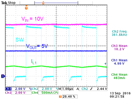
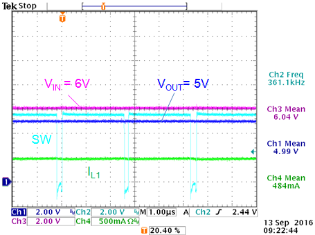
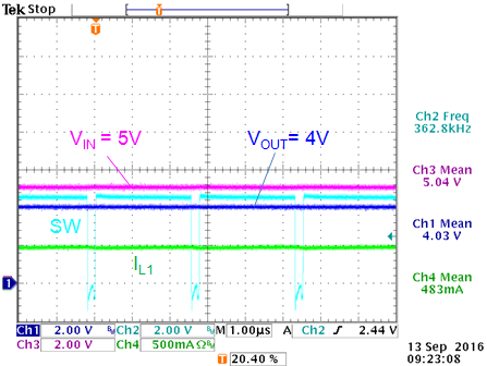
|
VIN = 10V: 50% duty-cycle
VOUT = 5V
|
VIN = 6V: close to max duty-cycle:
VOUT = 5V
|
VIN = 5V: dropout mode in max
duty-cycle operation. VOUT = 4V
|
|
|
|
|
Figure 14
The total 5V application schematic is shown in figure
15.
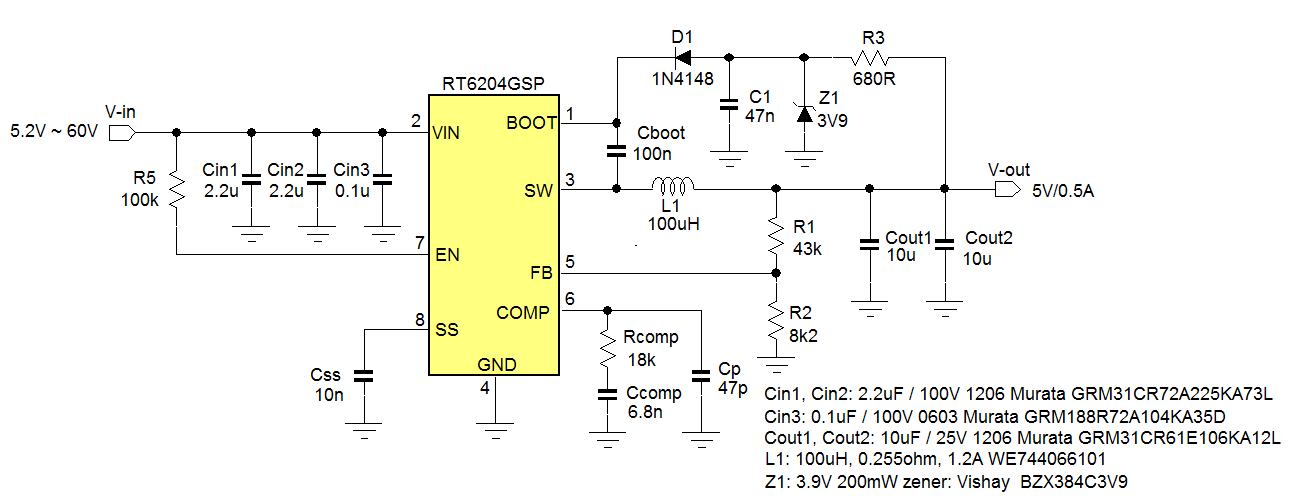
Figure 15
5. Third Example application: 12V output
The third example analyzes the converter with a
fixed 12V output and a wide input voltage range.
· The maximum input voltage for the 12V output case is the same as
for the 5V case: it is limited by the RT6204 60V maximum input voltage rating.
If the input supply can be lower than 18.5V, the duty-cycle will be higher
than 65%, and the external bootstrap charging circuit needs to be implemented.
· Feedback network: use
 to select R1 and R2: In this case we choose R1 = 140k and R2 = 10k as shown
in the datasheet.
to select R1 and R2: In this case we choose R1 = 140k and R2 = 10k as shown
in the datasheet.
· Inductor value: For this 12V application, the duty-cycle can exceed
50% when VIN is lower than 24V, so for wide VIN applications,
the effect of slope compensation on the minimum required inductance needs
to be considered. The slope compensation criteria
 requires an inductor greater than 200µH.
Inductor calculation based on 30% current ripple
at 60V input using
 gives L = 183µH. In this example we will use 220µH. The selected
inductor is Bourns SRU1048A-221Y shielded inductor with a 0.7A saturation current
and 0.455Ω resistance.
gives L = 183µH. In this example we will use 220µH. The selected
inductor is Bourns SRU1048A-221Y shielded inductor with a 0.7A saturation current
and 0.455Ω resistance.
· Output
capacitor choice: For this 12V application you could either choose ceramic
or electrolytic output capacitors. MLCC ceramic capacitors have considerable
capacitance drop due to 12V dc bias, and you’ll need larger case size MLCC
or several pieces in parallel to reach an effective capacitance above 10µF.
For example, the 10µF/25V X5R 1206 size MLCC GRM31CR61E106KA12L will
have around 2.9µF at 12Vdc and low ac ripple. Two pieces in parallel
will give 5.8µF.
A small SMD aluminum electrolytic capacitor of 47µF,
35V, 6.3x5.8mm size (like the Panasonic VFK Series) has an ESR of 0.36Ω
and a rated RMS current of 240mA. You can calculate the output ripple for
both types in PSM mode and CCM mode. The PSM peak current can be calculated
in a similar way as the 5V example, and will be around 165mA for a 60V –
12V application with a 220µH inductor. The CCM ripple current will
be around 124mApp.

PSM ripple at 60V input with 5.8µF MLCC output
capacitance will be around 55mVpp.
CCM ripple at 60V input with 5.8µF MLCC output
capacitance will be around 8mVpp.
PSM ripple at 60V input with 47µF electrolytic
capacitor with 0.36Ω ESR will be around 59mVpp.
CCM ripple at 60V input with 47µF electrolytic
capacitor with 0.36Ω ESR will be around 46mVpp.
As can be seen, the PSM output ripple for both types
of capacitor are quite close, but MLCC capacitors will have lower ripple
in CCM mode. But if you do the calculations at lower input voltage, you’ll
find that the electrolytic capacitor will have lower PSM ripple than the
MLCC capacitors.
For this 12V output example, we will use the 47µF/35V
6.3x5.8mm electrolytic capacitor with ESR 0.36Ω.
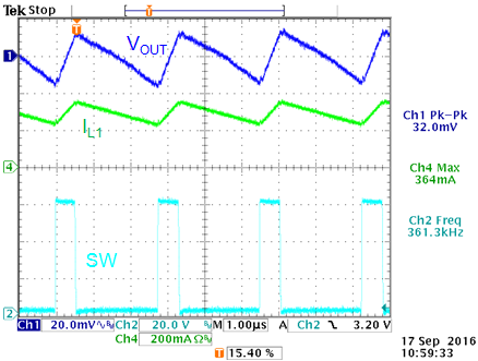
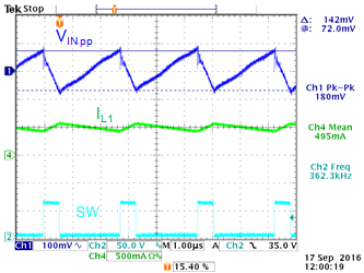
Figure 16 shows the measured output ripple in PSM
mode and CCM mode when using this electrolytic output capacitor.
|
12V output ripple in PSM mode with electrolytic
capacitor: Ripple voltage is 46mVpp
|
12V output ripple in CCM mode with electrolytic
capacitor: Ripple voltage is 32mVpp
|
|
|
|
Figure 16
It should be noted that electrolytic capacitor ESR
is heavily dependent on temperature: ESR becomes higher at lower temperatures.
This effect should be included when the power supply has to operate at lower
temperatures.
It is recommended to place a small 100nF/50V ceramic
capacitor in parallel with the electrolytic output capacitor: The low ESR
ceramic capacitor will filter the high frequency spikes from the switching
transitions. But this capacitor will not have any effect on the ripple amplitude
or converter stability.
· For the
input capacitor selection we’ll use the same values as were used in the
5V output example:
A small 100nF/100V 0603 X7R capacitor (Murata GRM188R72A104KA35)
in parallel with two pieces 2.2µF/100V 1206 X7R capacitor (Murata
GRM31CR72A225KA73) giving a total combination of 1.5µF.
From
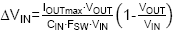 with a maximum 0.5A load current, 60V input and 12V output, 1.5µF
of input capacitance will give an input ripple of around 152mVpp.
with a maximum 0.5A load current, 60V input and 12V output, 1.5µF
of input capacitance will give an input ripple of around 152mVpp.
The worst case RMS current in the input capacitor
in this 12V application will happen when VIN is 24V and the load
is 0.5A. The maximum RMS current will be 0.25A; this will not be a problem
for the selected input capacitors.
|
|
Figure 17 shows the actual input ripple
measurement, which shows 142mV saw-tooth input ripple. Additional
high frequency noise is due to parasitic inductance.
|
|
Figure 17
|
|
· Calculation
of compensation components.
For the compensation component calculations we will
use the formulas as given in chapter 2. For the output capacitance we use
COUT = 47µF and Output capacitor ESR = 0.36Ω. We
will first use the standard bandwidth setting of 0.1 ‧ FSW:
 : With GmEA = 970µA/V, GCS = 0.9A/V and COUT
= 47µF: RCOMP becomes 178kΩ. We will choose
180kΩ.
: With GmEA = 970µA/V, GCS = 0.9A/V and COUT
= 47µF: RCOMP becomes 178kΩ. We will choose
180kΩ.
The converter load pole
 lies at 141Hz.
 = 6.3nF. We choose 6.8nF.
The output capacitor ESR of 0.36Ω will result
in an ESR zero of at 9.4kHz. From
 we can find that CP needs to be 95pF. We’ll choose 100pF.
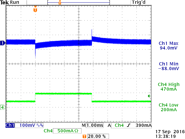
Figure 18 show the step load response at room temperature,
with a fast load step from 250mA to 500mA.
|
4msec step at 25oC: VOUT
recovery time around 3msec due to RCOMP ‧ CCOMP
time constant.
|
80µsec step shows the initial VOUT
drop due output cap ESR.
|
Zoom of ESR drop confirms the voltage drop
to be ΔILOAD ‧ ESR
(250mA ‧ 0.36Ω = 90mV)
|
|
|
|
|
Figure 18
As mentioned earlier, electrolytic capacitor ESR
is heavily dependent on temperature: ESR becomes much higher at lower temperatures.
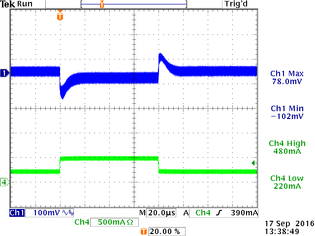
Below figure 19 show the step response at -20oC:
|
4msec step at -20oC; Increased
ripple.
|
80µsec step at -20oC shows
instability.
|
Zoom shows a voltage drop to be ΔILOAD ‧ ESR
to be 316mV:
ESR is now 316mV/250mA = 1.26Ω
|
|
|
|
|
Figure 19
Clearly the converter is not stable at lower temperatures.
What happened is that the increased output capacitor ESR at low temperature
sets the modulator ESR zero at much lower frequency, around 2.6kHz. This
increases the modulator gain at high frequencies and results in a much higher
control bandwidth. The phase margin will be poor.
To overcome this problem the compensation needs
to be adjusted: You could just increase the value of CP, but
this will reduce phase margin at room temperature ESR. It is better to reduce
the overall converter bandwidth by reducing RCOMP considerably.
This will give the best phase margin in both high ESR (low temperature)
and low ESR (high temperature) condition.
In this case we lower the bandwidth with a factor
3 to around 13kHz: RCOMP becomes 68k. CCOMP now becomes
15nF. Calculate CP for room temperature ESR of 0.36Ω: CP
becomes 250pF, choose 270pF. The figure 20 below show the result: The step
load response now looks good at both low temperature and high temperature
conditions.
|
Load step at +25oC : OK
|
Load step at -30oC : OK
|
Load step at +70oC : OK
|
|
|
|
|
Figure 20
· Soft-start
design: For the 12V application with 47µF output capacitance, too
fast VOUT rise time can result in some inrush current: To keep
the inrush during VOUT rise less than 100mA, the rise time must
be greater than 47µF ‧ 12V/100mA = 5.6msec.
 , so CSS needs to be larger than 42nF. We will choose 47nF. This
gives total start-up time of 8.6msec and VOUT rise time from
0 to 12V will be 6.3msec.
, so CSS needs to be larger than 42nF. We will choose 47nF. This
gives total start-up time of 8.6msec and VOUT rise time from
0 to 12V will be 6.3msec.
|
|
Figure 21 shows the soft-start behavior
of the 12V application.
|
|
Figure 21
|
|
| |
|
|
· External
Bootstrap capacitor charging circuit.
If the converter input can be lower than 18.5V,
the external bootstrap supply is needed. The optimal value for this bootstrap
supply is around 3.3V: Higher values like 5V can lead to too strong high-side
MOSFET drive which can lead to noise and unstable switching at certain conditions.
The 3.3V bootstrap supply can derived from the 12V output by using a zener
voltage clamp similar to the 5V application. With an average bootstrap charge
current of 1mA and a zener bias current of 1.5mA, the zener bias resistor
R3 becomes (12V-3.3V)/2.5mA = 3.5k. We will choose 3.3k. The total power dissipation
in R3 is 2.5mA2 ‧ 3.3kΩ = 20mW, so a small size SMD resistor
can be used. The circuit is shown in figure 22.
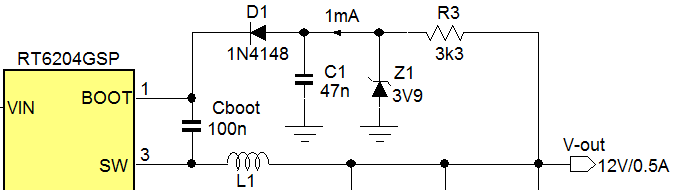
Figure 22
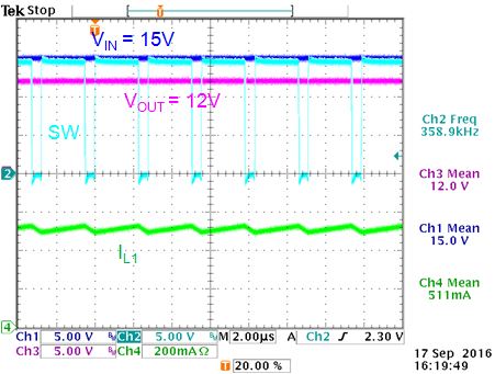
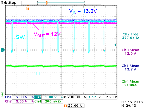
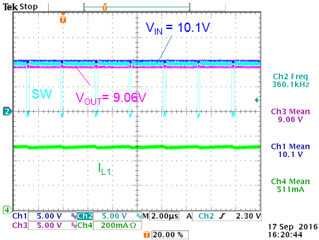
Figure 23 below shows the 12V converter operation
at maximum load when VIN is reduced: The maximum duty-cycle is
determined by the converter minimum off time which is around 200nsec, which
results in 93% max duty-cycle. The input voltage where the converter reaches
the max duty-cycle depends on load current: The I ‧ Rdson drop and inductor
I ‧ DCR drop need to be included, which is around 0.66V at 0.5A load for the
12V application. The VIN where drop-out starts to happen is then
12V/0.93 + 0.66V = 13.56V.
|
VIN = 15V: ~80% duty-cycle
VOUT = 12V
|
VIN = 13.3V: just at max duty-cycle:
VOUT = 12V
|
VIN = 10.1V: dropout mode in
max duty-cycle operation. VOUT = 9.06V
|
|
|
|
|
Figure 23
The total 12V application schematic is shown in
figure 24.
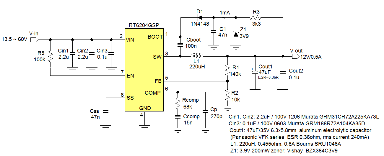
Figure 24
6. Fourth Example application: 24V output
This fourth example examines the converter with
a fixed 24V output and a wide input voltage range.
· The maximum input voltage for the 24V output case is the same as
for the 12V case: it is limited by the RT6204 60V maximum input voltage
rating. If the input supply can be lower than 37V, the duty-cycle will be
higher than 65%, and the external bootstrap charging circuit needs to be
implemented.
· Feedback network: use
 to select R1 and R2: In this case we choose R2 = 10k and R1 = 290k.
· Inductor value: For this 24V application, the duty-cycle can exceed
50% when VIN is lower than 48V, so for wide VIN applications,
the effect of slope compensation on the minimum required inductance needs
to be considered. The slope compensation criteria
 (µH) requires an inductor greater than 400µH.
Inductor calculation based on 30% current ripple
at 60V input using
 gives L = 274µH. So we need to select the inductor based on slope
compensation criteria. In this example we will use 470µH. The selected
inductor is Bourns SSR1240-471 shielded inductor with a 0.6A saturation
current and 1.35Ω resistance.
gives L = 274µH. So we need to select the inductor based on slope
compensation criteria. In this example we will use 470µH. The selected
inductor is Bourns SSR1240-471 shielded inductor with a 0.6A saturation
current and 1.35Ω resistance.
· Output
capacitor choice: For this 24V application, MLCC ceramic capacitors are
not really suitable due to their large capacitance drop at high DC bias
voltage. To achieve sufficient capacitance, you’d need large size 50V MLCC
types, which are quite expensive.
Small SMD aluminum electrolytic capacitors are more
suitable. In the 12V output application we used 47µF, 35V, 6.3x5.8mm
size (Panasonic VFK Series) with an ESR of 0.36Ω and a rated RMS current
of 240mA. We can consider using this capacitor for the 24V application as
well.
You can calculate the output ripple in PSM mode
and CCM mode. The PSM peak current for this 24V case will be the IC regulated
PSM peak value of 150mA, without much propagation delay influence. The CCM
ripple current with 470u inductor will be around 88mApp.
PSM ripple at 60V input with 47µF electrolytic
capacitor with 0.36Ω ESR will be around 62mVpp.
CCM ripple at 60V input with 47µF electrolytic
capacitor with 0.36Ω ESR will be around 32mVpp.
For this 24V output example, we will use the 47µF/35V
6.3x5.8mm electrolytic capacitor with ESR 0.36Ω.
Figure 25 shows the measured output ripple in PSM
mode and CCM mode when using this electrolytic output capacitor. It is recommended
to place a small 100nF/50V ceramic capacitor in parallel with the electrolytic
output capacitor: The low ESR ceramic capacitor will filter the high frequency
spikes from the switching transitions. But this capacitor will not have
any effect on the ripple amplitude or converter stability.
|
24V output ripple in PSM mode with electrolytic
capacitor: Ripple voltage is 82mVpp
|
24V output ripple in CCM mode with electrolytic
capacitor: Ripple voltage is 38mVpp
|
|
|
|
Figure 25
Input capacitor selection: The 24V application will
have higher input ripple than the previous examples since the power level
is higher. In the 12V application we used the 100nF/100V 0603 X7R capacitor
(Murata GRM188R72A104KA35) in parallel with two pieces 2.2µF/100V
1206 X7R capacitor (Murata GRM31CR72A225KA73) giving a total combination
of 1.5µF.
If we use this same combination in the 24V application
with 60V input and 0.5A load:
 will give an input ripple of around 229mVpp. For EMC reasons, it may be
necessary to add an additional 2.2µF/100V 1206 X7R and a high frequency
bead.
will give an input ripple of around 229mVpp. For EMC reasons, it may be
necessary to add an additional 2.2µF/100V 1206 X7R and a high frequency
bead.
|
|
Figure 26 shows the actual input ripple
measurement with the same 1.5µF input capacitor, resulting
in a 230mVpp saw-tooth input ripple at 60V input and max 0.5A load.
The worst case RMS current in the input
capacitor in this 24V application will happen when VIN
is 48V and the load is 0.5A. The maximum RMS current will be 0.25A.
This will not be a problem for the selected input capacitors.
|
|
Figure 26
|
|
· Calculation
of compensation components.
As was shown in the 12V output application, the
electrolytic output capacitor ESR variation over temperature can have a
big impact on converter stability. If the converter has to work at very
low temperatures, a factor 3 higher ESR has to be considered. Due to this
effect, the converter bandwidth has to be set a factor 3 lower than the
standard 0.1 ‧ FSW setting. For the 24V output supply, we will
use similar bandwidth as the 12V application, around 12kHz instead of 35kHz.
For the compensation component calculations we will use the formulas as
given in chapter 2. For the output capacitance we use COUT =
47µF and output capacitor ESR = 0.36Ω.
 :
With GmEA = 970µA/V, GCS = 0.9A/V and COUT
= 47µF: RCOMP becomes 124kΩ. We will choose 120kΩ.
:
With GmEA = 970µA/V, GCS = 0.9A/V and COUT
= 47µF: RCOMP becomes 124kΩ. We will choose 120kΩ.
The converter load pole
 lies at 71Hz.
 = 18.7nF. We choose 18nF.
We use the room temperature ESR to calculate CP:
The output capacitor ESR of 0.36Ω will result in an ESR zero of at
9.4kHz. When we calculate
 we can find that CP needs to be 136pF. We’ll choose a slightly
larger value of 150pF.
we can find that CP needs to be 136pF. We’ll choose a slightly
larger value of 150pF.
Figures 27 show the 250mA to 500mA step load response
at +25oC (longer duration), and short duration pulse load steps
at -30oC and +70oC to see the details of the transition.
|
12msec load step at +25oC
|
120µsec load step at -30oC
: OK
|
120µsec load step at +70oC
: OK
|
|
|
|
|
Figure 27
· Soft-start
design: To keep the inrush current below 100mA for the 24V application with
47µF output capacitance, the VOUT rise time must be larger
than 47µF ‧ 24V/100mA = 11msec.
 ,
so CSS needs to be larger than 82nF. We will choose 100nF. VOUT
rise time from 0 to 24V will be 13msec.
,
so CSS needs to be larger than 82nF. We will choose 100nF. VOUT
rise time from 0 to 24V will be 13msec.
|
|
Figure 28 shows the soft-start behavior
of the 24V application.
|
|
Figure 28
|
|
· External
Bootstrap capacitor charging circuit.
If the converter input can be lower than 37V, the
external bootstrap supply is needed. The optimal value for this bootstrap
supply is around 3.3V: Higher values like 5V can lead to too strong high-side
MOSFET drive which can lead to noise and unstable switching at certain conditions.
The 3.3V bootstrap supply can derived from the 24V output by using a zener
voltage clamp similar to the 12V application.
With an average bootstrap charge current of 1mA
and a zener bias current of 1.5mA, the zener bias resistor R3 becomes (24-3.3)/2.5mA
= 8.2k. The total power dissipation in R3 is 2.5mA2 ‧ 8.2kΩ
= 51mW, which may require a slightly larger size SMD resistor. The circuit
is shown in figure 29.
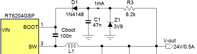
Figure 29
Figure 30 below shows the 24V converter operation
at maximum load when VIN is reduced: The maximum duty-cycle is
determined by the converter minimum off time which is around 200nsec, which
results in 93% max duty-cycle. The input voltage where the converter reaches
the max duty-cycle depends on load current: The I ‧ Rdson drop and inductor
I ‧ DCR drop need to be included, which is around 0.98V at 0.5A load for the
24V application. For the 24V application at 0.5A load current, the VIN
where drop-out starts to happen is then 24V/0.93 + 0.98V = 26.8V.
|
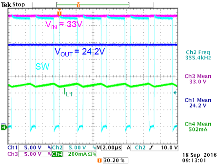
VIN = 33V: ~75% duty-cycle
VOUT = 24.2V
|
VIN = 27.3V: just at max duty-cycle:
VOUT = 24.2V
|
VIN = 25.2V: dropout mode in
max duty-cycle operation. VOUT = 22.2V
|
|
|
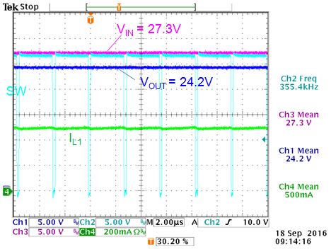
|
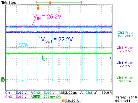
|
Figure 30
The total 24V application schematic is shown in
figure 31.
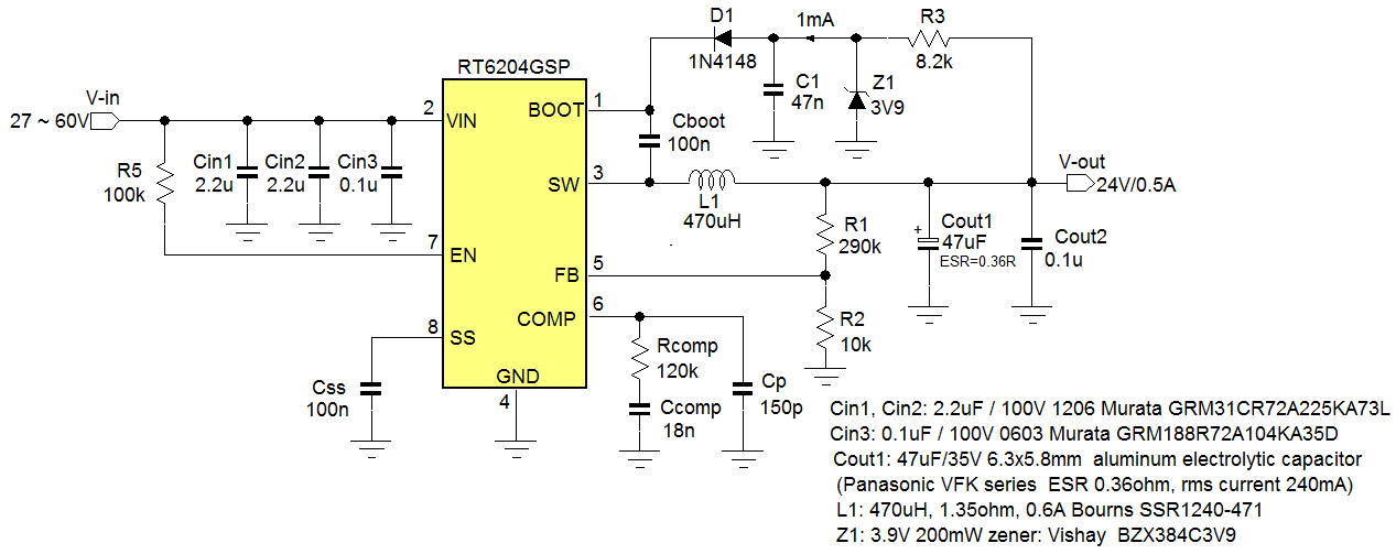
Figure 31
7. Conclusion
RT6204 buck converter can be successfully used in
applications that require wide input range and wide output range. The external
compensation and soft-start make it possible to tune the design for various
types of output capacitors. Simple formulas can be used to determining the
external key components and measured results match the calculated results
quite well.